- 您现在的位置:买卖IC网 > Sheet目录471 > MAX2023ETX+T (Maxim Integrated)IC MOD/DEMOD HI DYN RNG 36-TQFN
�� �
�
�High-Dynamic-Range,� Direct� Up-/Downconversion�
�1500MHz� to� 2500MHz� Quadrature� Mod/Demod�
�The� I/Q� input� power� levels� and� the� insertion� loss� of� the�
�device� determine� the� RF� output� power� level.� The� input�
�power� is� a� function� of� the� delivered� input� I� and� Q� volt-�
�ages� to� the� internal� 50� Ω� termination.� For� simple� sinu-�
�soidal� baseband� signals,� a� level� of� 89mV� P-P� differential�
�on� the� I� and� the� Q� inputs� results� in� a� -17dBm� input�
�power� level� delivered� to� the� I� and� Q� internal� 50� Ω� termi-�
�nations.� This� results� in� an� RF� output� power� of� -26.6dBm.�
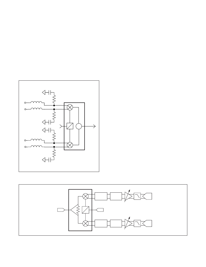
�C� =� 2.2pF�
�External� Diplexer�
�LO� leakage� at� the� RF� port� can� be� nulled� to� a� level� less�
�than� -80dBm� by� introducing� DC� offsets� at� the� I� and� Q�
�ports.� However,� this� null� at� the� RF� port� can� be� compro-�
�mised� by� an� improperly� terminated� I/Q� IF� interface.� Care�
�must� be� taken� to� match� the� I/Q� ports� to� the� driving� DAC�
�circuitry.� Without� matching,� the� LO’s� second-order� (2f� LO� )�
�term� may� leak� back� into� the� modulator’s� I/Q� input� port�
�where� it� can� mix� with� the� internal� LO� signal� to� produce�
�additional� LO� leakage� at� the� RF� output.� This� leakage�
�effectively� counteracts� against� the� LO� nulling.� In� addi-�
�tion,� the� LO� signal� reflected� at� the� I/Q� IF� port� produces� a�
�residual� DC� term� that� can� disturb� the� nulling� condition.�
�50� Ω�
�MAX2023�
�RF� MODULATOR�
�As� demonstrated� in� Figure� 3,� providing� an� RC� termination�
�on� each� of� the� I+,� I-,� Q+,� Q-� ports� reduces� the� amount� of�
�I�
�L� =� 11nH�
�50� Ω�
�LO� leakage� present� at� the� RF� port� under� varying� temper-�
�ature,� LO� frequency,� and� baseband� termination� condi-�
�tions.� See� the� Typical� Operating� Characteristics� for�
�details.� Note� that� the� resistor� value� is� chosen� to� be� 50� Ω�
�with� a� corner� frequency� 1� /� (2� π� RC)� selected� to� adequate-�
�C� =� 2.2pF�
�LO�
�0� °�
�90� °�
�∑�
�RF�
�ly� filter� the� f� LO� and� 2f� LO� leakage,� yet� not� affecting� the� flat-�
�ness� of� the� baseband� response� at� the� highest� baseband�
�frequency.� The� common-mode� f� LO� and� 2f� LO� signals� at�
�50� Ω�
�I+/I-� and� Q+/Q-� effectively� see� the� RC� networks� and� thus�
�become� terminated� in� 25� Ω� (R/2).� The� RC� network� pro-�
�vides� a� path� for� absorbing� the� 2f� LO� and� f� LO� leakage,�
�Q�
�L� =� 11nH�
�C� =� 2.2pF�
�50� Ω�
�while� the� inductor� provides� high� impedance� at� f� LO� and�
�2f� LO� to� help� the� diplexing� process.�
�RF� Demodulator�
�The� MAX2023� can� also� be� used� as� an� RF� demodulator�
�(see� Figure� 4),� downconverting� an� RF� input� signal�
�directly� to� baseband.� The� single-ended� RF� input�
�accepts� signals� from� 1500MHz� to� 2500MHz� with� power�
�Figure� 3.� Diplexer� Network� Recommended� for� DCS� 1800/�
�PCS� 1900� EDGE� Transmitter� Applications�
�levels� up� to� +30dBm.� The� passive� mixer� architecture�
�produces� a� conversion� loss� of� typically� 9.5dB.� The�
�MAX2023�
�DIPLEXER/�
�DC� RETURN�
�MATCHING�
�ADC�
�RF�
�90�
�0�
�LO�
�DIPLEXER/�
�DC� RETURN�
�MATCHING�
�ADC�
�Figure� 4.� MAX2023� Demodulator� Configuration�
�13�
�发布紧急采购,3分钟左右您将得到回复。
相关PDF资料
MAX2027EUP+D
IC AMP VAR GAIN 20-TSSOP
MAX2027EVKIT
EVAL KIT FOR MAX2027
MAX2029ETP+T
IC MIXER UP/DOWN HI LIN 20-TQFN
MAX2031EVKIT
EVAL KIT FOR MAX2031
MAX2032ETP+
IC MIXER UP/DOWN CONVER 20TQFN
MAX2034CTM+
IC AMP LOW NOISE QUAD 48-TQFN
MAX2035EVKIT
EVAL KIT FOR MAX2035
MAX2039ETP+D
IC MIXER UP/DWN HI LIN 20-TQFN
相关代理商/技术参数
MAX2023ETX-T
功能描述:调节器/解调器 1.5GHz-2.3GHz Quad Mod/Demod RoHS:否 制造商:Texas Instruments 封装 / 箱体:PVQFN-N24 封装:Reel
MAX2023EVKIT
功能描述:调节器/解调器 Hi-Dynamic-Range Direct Upconversion 1500MHz - 2300MHz Quadrature Mod/Dem RoHS:否 制造商:Texas Instruments 封装 / 箱体:PVQFN-N24 封装:Reel
MAX2023EVKIT+
功能描述:调节器/解调器 MAX2023 Evaluation Kit RoHS:否 制造商:Texas Instruments 封装 / 箱体:PVQFN-N24 封装:Reel
MAX20-24.0C
制造商:MDE 制造商全称:MDE Semiconductor, Inc. 功能描述:HIGH CURRENT TRANSIENT VOLTAGE SUPPRESSOR (TVS) DIODE
MAX20-24.0CA
制造商:MDE 制造商全称:MDE Semiconductor, Inc. 功能描述:HIGH CURRENT TRANSIENT VOLTAGE SUPPRESSOR (TVS) DIODE
MAX20-26.0C
制造商:MDE 制造商全称:MDE Semiconductor, Inc. 功能描述:HIGH CURRENT TRANSIENT VOLTAGE SUPPRESSOR (TVS) DIODE
MAX20-26.0CA
制造商:MDE 制造商全称:MDE Semiconductor, Inc. 功能描述:HIGH CURRENT TRANSIENT VOLTAGE SUPPRESSOR (TVS) DIODE
MAX2027
制造商:MAXIM 制造商全称:Maxim Integrated Products 功能描述:Evaluation Kit